From inside (document excerpt):
CONTENTS SPECiFiCATIONS. 2 CIRCUIT DESCRIPTION . ALIGNMENT PARTS LiST SEMICONDUCTOR OAT A EXPLODED ViEW COMPONENT LOCATOR . BLOCK DIAGRAM SCHEMATIC DIAGRAM 5 6 9 14 16 20 21 AL.’NCO, INC. Information in this document are subject to change without notice or obligation. All brand names and trademarks are the propeny of their respective owners. Alinco cannot be liable for pictorial or typographical inaccuracIes.
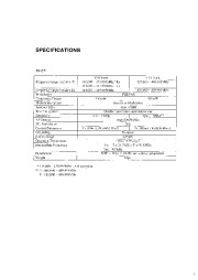
Some parts, options and/or accessories are unavailable in cenain areas. Changes or modifications not expressly approved by the pany responsible for compliance could void the user’s authority to operate the equipment. 1998 No part of this document may be reproduced, copied, translated or transcribed in any fom1 or by any means without the prior written permission of Alinco, Inc., Osaka, Japan. English Edition Printed in Japan SPECIFICATIONS DJ-C5 Frequency range (version -T) Frequency range (version -E) Modulation Transmitter Output Modulation system Spurious ratio Receiver system Sensitivity AF Output Mic Impedance Current Dissipation Grounding Rated voltage Operating Temperature Intermediate Frequency Dimensions Weight YHFband 118.000 173.995MHz *Rx 144.000 – 147.995MHz Tx 144.000 – 145.995MHz F3E(FM) 300mW Reactance Modulation max – 60dB Double-conversion superheterodyne max – 15dB ** max – 16dB max 60mW(8Q) 2kQ Tx 240mA / Rx(BS) 30mA Tx 300mA / Rx(BS) 40mA Negative 3.8YDC – 10 to + 50 deg.C 1st T = 21.7MHz / E = 20.8MHz 2nd 450kHz 56W X 94H X 1O.6D mm without projections 85gr. 350mW UHF band 420.000 449.995MHz 430.000 439.995MHz * 118.000 – 135.995MHz : AM reception ** T : 440.000 – 449.995MHz E : 430.000 – 439.995MHz


 Alinco DJ-C5 SM VHF UHF FM Radio Instruction Owners Manual - 1 of 26
 Alinco DJ-C5 SM VHF UHF FM Radio Instruction Owners Manual - 2 of 26
 Alinco DJ-C5 SM VHF UHF FM Radio Instruction Owners Manual - 3 of 26
 Alinco DJ-C5 SM VHF UHF FM Radio Instruction Owners Manual - 4 of 26
 Alinco DJ-C5 SM VHF UHF FM Radio Instruction Owners Manual - 5 of 26
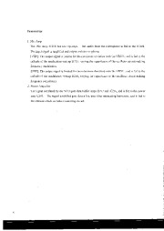 Alinco DJ-C5 SM VHF UHF FM Radio Instruction Owners Manual - 6 of 26
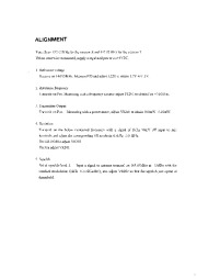 Alinco DJ-C5 SM VHF UHF FM Radio Instruction Owners Manual - 7 of 26
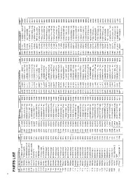 Alinco DJ-C5 SM VHF UHF FM Radio Instruction Owners Manual - 8 of 26
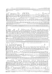 Alinco DJ-C5 SM VHF UHF FM Radio Instruction Owners Manual - 9 of 26
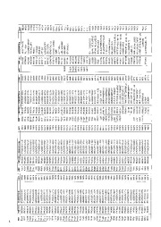 Alinco DJ-C5 SM VHF UHF FM Radio Instruction Owners Manual - 10 of 26